
While TSMC formally started mass production of chips on its N3 (3nm-class) process technology late last year, the company is set to finally ship the first revenue wafers in the current quarter. During the most recent earnings call with analysts and investors, the company said that demand for 3 nm products was steady, and that numerous designs for smartphones and high-performance applications are incoming later this year. Furthermore, N3E manufacturing node is on track for high-volume manufacturing later this year.
“We are seeing robust demand for N3 and we expect a strong ramp of N3 in the second half of this year, supported by both HPC and smartphone applications,” said C.C. Wei, chief executive officer of TSMC, during the company’s earnings. Call with financial analysts and investors.
Previously the company never commented on applications that use its initial N3 fabrication process, but for now it actually disclosed that devices that are in mass production are designed for smartphones as well as HPC applications, which is a vague term which TSMC uses to describe everything from handheld game consoles all the way to heavy-duty smartphone SoCs.
For customer privacy reasons, TSMC does not disclose which customers are using N3. Though historically, Apple has been TSMC’s alpha client for its leading-edge process technologies, so they’re the most likely candidate to be the biggest consumer of TSMC’s N3 output.
TSMC’s baseline N3 node (aka N3B) is an expensive technology to use. It features up to 25 EUV layers (according to China Renaissance and SemiAnalysis) with TSMC using EUV double-patterning on some of them to make for higher logic and SRAM transistor density than N5. EUV steps are expensive in general, and EUV double patterning drives those costs up further, which is why this fabrication process is only expected to be used by a handful of customers who are not as concerned about the high expenditure required.
For those who are more cost sensitive, there is N3E, which can ‘only’ use up to 19 EUV layers and does not use EUV double patterning. Good news is that TSMC expects to commence mass production on this node to Q4 2023.
N3E has passed qualification and achieved performance and yield target and will start volume production in the fourth quarter of this year,” said Wei.
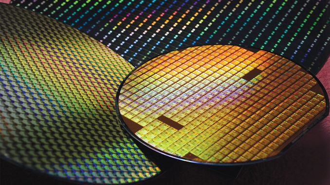
Source: TSMC