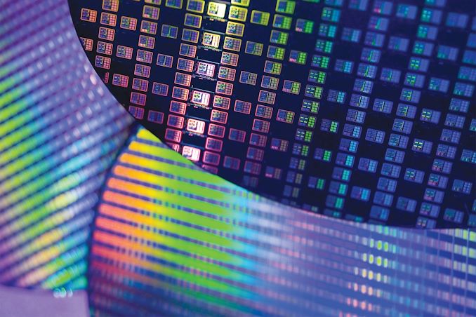

Speaking to partners last week as part of their annual Open Innovation Platform forum in Europe, a big portion of TSMC’s roadshow was dedicated to the next generation of the company’s foundry technology. TSMC’s 2 nm-class N2, N2P, and N2X process technologies are set to introduce multiple innovations, including nanosheet gate-all-around (GAA) transistors, backside power delivery, and super-high-performance metal-insulator-metal (SHPMIM) capacitor over the next few years. But in order to take advantage of these innovations, TSMC warns, chip designers will need to use all-new electronic design automation (EDA), simulation, and verification tools as well as IP. And while making such a big shift is never an easy task, TSMC is bringing some good news to chip designers early-on: even with N2 still a couple of years out, many of the major EDA tools, verification tools, foundation IP, and even analog IP for N2 are already available for use.
“For N2 we could be working with them two years in advance already because nanosheet is different,” said Dan Kochpatcharin, Head of Design Infrastructure Management at TSMC, at the OIP 2023 conference in Amsterdam. “[EDA] tools have to be ready, so what the OIP did is to work with them early. We have a huge engineering team to work with the EDA partners, IP partners, [and other] partners.”
| Advertised PPA Improvements of New Process Technologies Data announced during conference calls, events, press briefings and press releases |
|||||
| TSMC | |||||
| N5 vs N7 |
N3 vs N5 |
N3E vs N5 |
N2 vs N3E |
||
| Power | -30% | -25-30% | -34% | -25-30% | |
| Performance | +15% | +10-15% | +18% | +10-15% | |
| Chip Density* | ? | ? | ~1.3X | >1.15X | |
| Volume Manufacturing |
Q2 2022 | H2 2022 | Q2/Q3 2023 | H2 2025 | |
*Chip density published by TSMC reflects ‘mixed’ chip density consisting of 50% logic, 30% SRAM, and 20% analog.
Preparations for the start of N2 chip production, scheduled for sometime in the second half of 2025, began long ago. Nanosheet GAA transistors behave differently than familiar FinFETs, so EDA and other tool and IP makers had to build their products from scratch. This is where TSMC’s Open Innovation Platform (OIP) demonstrated its prowess and enabled TSMC’s partners to start working on their products well in advance.
By now, major EDA tools from Cadence and Synopsys as well as many tools from Ansys and Siemens EDA have been certified by TSMC, so chip developers can already use them to design chips. Also, EDA software programs from Cadence and Synopsys are ready for analog design migration. Furthermore, Cadence’s EDA tools already support N2P’s backside power delivery network.
With pre-built IP designs, things are taking a bit longer. TSMC’s foundation libraries and IP, including standard cells, GPIO/ESD, PLL, SRAM, and ROM are ready both for mobile and high-performance computing applications. Meanwhile, some PLLs exist in pre-silicon development kits, whereas others are silicon proven. Finally, blocks such as non-volatile memory, interface IP, and even chiplet IP are not yet available – bottlenecking some chip designs – but these blocks in active development or planned for development by companies like Alphawave, Cadence, Credo, eMemory, GUC, and Synopsys, according to a TSMC slide. Ultimately, the ecosystem of tools and libraries for designing 2 nm chips is coming together, but it’s not all there quite yet.
“[Developing IP featuring nanosheet transistors] is not harder, but it does take more cycle time, cycle time is a bit longer,” said Kochpatcharin. “Some of these IP vendors also need to be trained [because] it is just different. To go from planar [transistor] to FinFET, is not harder, you just need to know how to do the FinFET. [It is] same thing, you just need to know how to do [this]. So, it does take some to be trained, but [when you are trained], it is easy. So that is why we started early.”
Although many of the major building blocks for chips are N2-ready, a lot of work still has to be done by many companies before TSMC’s 2 nm-class process technologies go into mass production. Large companies, which tend to design (or co-design) IP and development tools themselves are already working on their 2 nm chips, and should be ready with their products by the time mass production starts in 2H 2025. Other players can also fire up their design engines because 2 nm preps are well underway at TSMC and its partners.