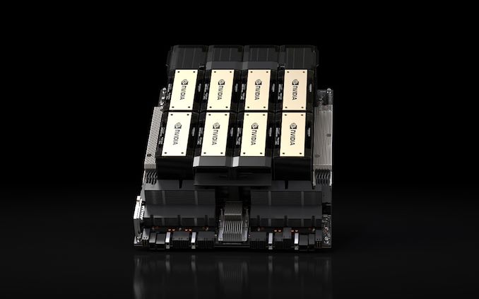
With faster and higher capacity HBM3E memory set to come online early in 2024, NVIDIA has been preparing its current-generation server GPU products to use the new memory. Back in August we saw NVIDIA’s plans to release an HBM3E-equipped version of the Grace Hopper GH200 superchip, and now for the SC23 tradeshow, NVIDIA is announcing their plans to bring to market an updated version of the stand-alone H100 accelerator with HBM3E memory, which the company will be calling the H200.
Like its Grace Hopper counterpart, the purpose of the H200 is to serve as a mid-generation upgrade to the Hx00 product line by rolling out a version of the chip with faster and higher capacity memory. Tapping the HBM3E memory that Micron and others are set to roll out n, NVIDIA will be able to offer accelerators with better real-world performance in memory bandwidth-bound workloads, but also parts that can handle even larger workloads. This stands to be especially helpful in the generative AI space – which has been driving virtually all of the demand for H100 accelerators thus far – as the largest of the large language models can max out the 80GB H100 as it is.
Meanwhile, with HBM3E memory not shipping until next year, NVIDIA has been using the gap to announce HBM3E updated parts at their leisure. Following this summer’s GH200 announcement, it was only a matter of time until NVIDIA announced a standalone version of the Hx00 accelerator with HBM3E, and this week NVIDIA is finally making that announcement.
| NVIDIA Accelerator Specification Comparison | |||||
| H200 | H100 | A100 (80GB) | |||
| FP32 CUDA Cores | 16896? | 16896 | 6912 | ||
| Tensor Cores | 528? | 528 | 432 | ||
| Boost Clock | 1.83GHz? | 1.83GHz | 1.41GHz | ||
| Memory Clock | ~6.5Gbps HBM3E | 5.24Gbps HBM3 | 3.2Gbps HBM2e | ||
| Memory Bus Width | 6144-bit | 5120-bit | 5120-bit | ||
| Memory Bandwidth | 4.8TB/sec | 3.35TB/sec | 2TB/sec | ||
| VRAM | 141GB | 80GB | 80GB | ||
| FP64 Vector | 33.5 TFLOPS? | 33.5 TFLOPS | 9.7 TFLOPS | ||
| INT8 Tensor | 1979 TOPS? | 1979 TOPS | 624 TOPS | ||
| FP16 Tensor | 989 TFLOPS? | 989 TFLOPS | 312 TFLOPS | ||
| FP64 Tensor | 66.9 TFLOPS? | 66.9 TFLOPS | 19.5 TFLOPS | ||
| Interconnect | NVLink 4 18 Links (900GB/sec) |
NVLink 4 18 Links (900GB/sec) |
NVLink 3 12 Links (600GB/sec) |
||
| GPU | GH100 (814mm2) |
GH100 (814mm2) |
GA100 (826mm2) |
||
| Transistor Count | 80B | 80B | 54.2B | ||
| TDP | 700W | 700W | 400W | ||
| Manufacturing Process | TSMC 4N | TSMC 4N | TSMC 7N | ||
| Interface | SXM5 | SXM5 | SXM4 | ||
| Architecture | Hopper | Hopper | Ampere | ||
Based on the same GH100 GPU as found in the original H100, the new HBM3E-equipped version of the H100 accelerator will be getting a new model number, H200, to set it apart from its original predecessor and align it with the GH200 superchip (whose HBM3E version is not getting a distinct model number).
Looking at the specifications being disclosed today, the H200 basically looks like the Hopper half of GH200 as its own accelerator. The big difference here, of course, is swapping out HBM3 for HBM3E, which is allowing NVIDIA to boost both memory bandwidth and capacity – as well as NVIDIA enabling the 6th HBM memory stack, which was disabled in the original H100. This will boost the H200’s memory bandwidth from 80GB to 141GB, and memory bandwidth from 3.35TB/second to what NVIDIA is preliminarily expecting to be 4.8TB/second.
Working backwards here based on total bandwidth and memory bus width, this indicates that H200’s memory will be running at roughly 6.5Gbps/pin, a roughly 25% frequency increase versus the original H100’s 5.3Gbps/pin HBM3 memory. This is actually well below the memory frequencies that HBM3E is rated for – Micron wants to hit 9.2Gbps/pin – but since it’s being retrofitted to an existing GPU design, it’s not surprising to see that NVIDIA’s current memory controllers don’t have the same range.
The H200 will also keep GH200’s unusual memory capacity of 141GB. The HBM3E memory itself physically has a capacity of 144GB – coming in the form of six 24GB stacks – however NVIDIA is holding back some of that capacity for yield reasons. As a result, customers don’t get access to all 144GB on board, but compared to H100 they are getting access to all six stacks, with the capacity and memory bandwidth benefits thereof.
As we’ve noted in past articles, shipping a part with all 6 working stacks will essentially require a perfect chip, as H100’s specs very generously allowed NVIDIA to ship parts with a non-functional stack. So this is likely to be a lower volume, lower yielding part than comparable H100 accelerators (which are already in short supply).
Otherwise, nothing NVIDIA has disclosed so far indicates that H200 will have better raw computational throughput than its predecessor. While real-world performance should improve from the memory changes, the 32 PFLOPS of FP8 performance that NVIDIA is quoting for an HGX H200 cluster is identical to the HGX H100 clusters available on the market today.
Finally, as with HBM3E-equipped GH200 systems, NVIDIA is expecting H200 accelerators to be available in the second quarter of 2024.
HGX H200 Announced: Compatible With H100 Systems
Alongside the H200 accelerator, NVIDIA is also announcing their HGX H200 platform, an updated version of the 8-way HGX H100 that uses the newer accelerator. The true backbone of NVIDIA’s H100/H200 family, the HGX carrier boards house 8 SXM form factor accelerators linked up in a pre-arranged, fully-connected topology. The stand-alone nature of the HGX board allows it to be plugged in to suitable host systems, allowing OEMs to customize the non-GPU parts of their high-end servers.
Given that HGX goes hand-in-hand with NVIDIA’s server accelerators, the announcement of the HGX 200 is largely a formality. Still, NVIDIA is making sure to announce it at SC23, as well as making sure that HGX 200 boards are cross-compatible with H100 boards. So server builders can use HGX H200 in their current designs, making this a relatively seamless transition.
Quad GH200 Announced: 4 GH200s Baked Into a Single Board
With NVIDIA now shipping both Grace and Hopper (and Grace Hopper) chips in volume, the company is also announcing some additional products using those chips. The latest of which is a 4-way Grace Hopper GH200 board, which NVIDIA is simply calling the Quad GH200.
Living up to the name, the Quad GH200 places four GH200 accelerators on to a single board, which can then be installed in larger systems. The individual GH200s are wired up to each other in an 8-chip, 4-way NVLink topology, with the idea being to use these boards as the building blocks for larger systems.
In practice, the Quad GH200 is the Grace Hopper counterpart to the HGX platforms. The inclusion of Grace CPUs technically makes each board independent and self-supporting, unlike the GPU-only HGX boards, but the need to connect them to host infrastructure remains unchanged.
A Quad GH200 node will offer 288 Arm CPU cores and a combined 2.3TB of high-speed memory. Notably, NVIDIA does not mention using the HBM3E version of GH200 here (at least not initially), so these figures seem to be with the original, HBM3 version. Which means we’re looking at 480GB of LPDDR5X per Grace CPU, and 96GB of HBM3 per Hopper GPU. Or a total of 1920GB of LPDDR5X and 384GB of HBM3 memory.
Jupiter Supercomputer: 24K GH200s at 18.2 Megawatts, Installing in 2024
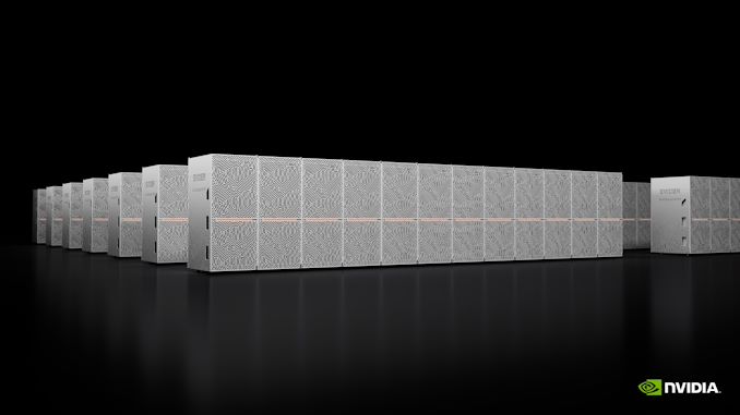
Finally, NVIIDA is announcing a new supercomputer design win this morning with Jupiter. Ordered by the EuroHPC Joint Undertaking, Jupiter will be a new supercomputer build out of 23,762 GH200 nodes. Once it comes online, Jupiter will be the largest Hopper-based supercomputer announced thus far, and is the first one that is explicitly (and publicly) targeting standard HPC workloads as well as the low-precision tensor-driven AI workloads that have come to define Hopper-based supercomputers announced thus far.
Contracted to Eviden and ParTec, Jupiter is a showcase of NVIDIA technologies through and through. Based on the Quad GH200 node that NVIDIA is also announcing today, Grace CPUs and Hopper GPUs sit at the core of the supercomputer. The individual nodes are backed by a Quantum-2 InfiniBand network, no doubt based on NVIDIA’s ConnectX adapters.
The company is not disclosing specific core count or memory capacity figures, but since we know what a single Quad GH200 board offers, the math is simple enough. At the top end (assuming no salvaging/binning for yield reasons), this would be 23,762 Grace CPUs, 23,762 Hopper H100-class GPUs, and roughly 10.9 PB of LPDDR5X and anther 2.2PB of HBM3 memory.
The system is slated to offer 93 EFLOPS of low-precision performance for AI uses, or over 1 EFLOPS of delivered high-precision (FP64) performance for traditional HPC workloads. The latter figure is especially notable, as that would make Jupiter the first NVIDIA-based exascale system for HPC workloads.
That said, NVIDIA’s HPC performance claims should be taken with a word of caution, as NVIDIA is still counting tensor performance here – 1 TFLOPS is just a bit under what 23,762 H100s can provide with FP64 tensor operations. The traditional metric for theoretical HPC supercomputer throughput is vector performance rather than matrix performance, so this figure isn’t entirely comparable to other systems. Still, with HPC workloads also making significant use of matrix math in parts, it’s not an entirely irrelevant claim, either. Otherwise, for anyone looking for the obligatory Frontier comparison, the straight vector performance of Jupiter would be around 800 TFLOPS, versus over twice that for Frontier. How close the two systems get in real-world conditions, on the other hand, will come down to how much matrix math is used in their respective workloads (LINPACK results should be interesting).
No price tag has been announced for the system, but power consumption has: a toasty 18.2 Megawatts of electricity (~3MW less than Frontier). So whatever the true price of the system is, like the system itself, it will be anything but petite.
According to NVIDIA’s press release, the system will be housed at the Forschungszentrum Jülich facility in Germany, where it will be used for “the creation of foundational AI models in climate and weather research, material science, drug discovery, industrial engineering and quantum computing.” Installation of the system is scheduled for 2024, though no date has been announced for when it’s expected to come online.


